Hole-Carrier-Dominant Transport in 2D Single-Crystal Copper

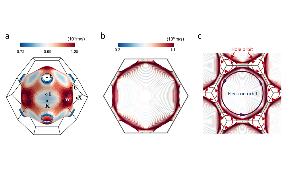
In 2D noble metals like copper, the carrier scattering at grain boundaries has obscured the intrinsic nature of electronic transport. However, it is demonstrated that the intrinsic nature of transport by hole carriers in 2D copper can be revealed by growing thin films without grain boundaries. Only when the grain boundaries are eliminated thoroughly, the hidden hole-like attribute of 2D single-crystal copper can be unmasked. Two types of Fermi surfaces, a large hexagonal Fermi surface centered at the zone center and the triangular Fermi surface around the zone corner, tightly matching to the calculated Fermi surface topology, confirmed by angle-resolved photoemission spectroscopy (ARPES) measurements and vivid nonlinear Hall effects of the 2D single-crystal copper account for the presence of hole carriers experimentally. This breakthrough suggests the potential to manipulate the majority carrier polarity in metals by means of grain boundary engineering in a 2D geometry.
* Reference
- Authors (Pusan National University)
· 1st author: Jong Mok Ok(Department of Physics)
· Corresponding author: Se-Young Jeong(Department of Optics and Mechatronics Engineering, Engineering Research Center for Color-Modulated Extra-Sensory Perception Technology)
- Title of original paper: Hole-Carrier-Dominant Transport in 2D Single-Crystal Copper
- Journal: Advanced Materials

 936 정세영옥종목교수1.jpg
(295KB)