Van der Waals integration of 1D Nb2Pd3Se8 and 2D WSe2 for gate-tunable in-sensor imaging processing

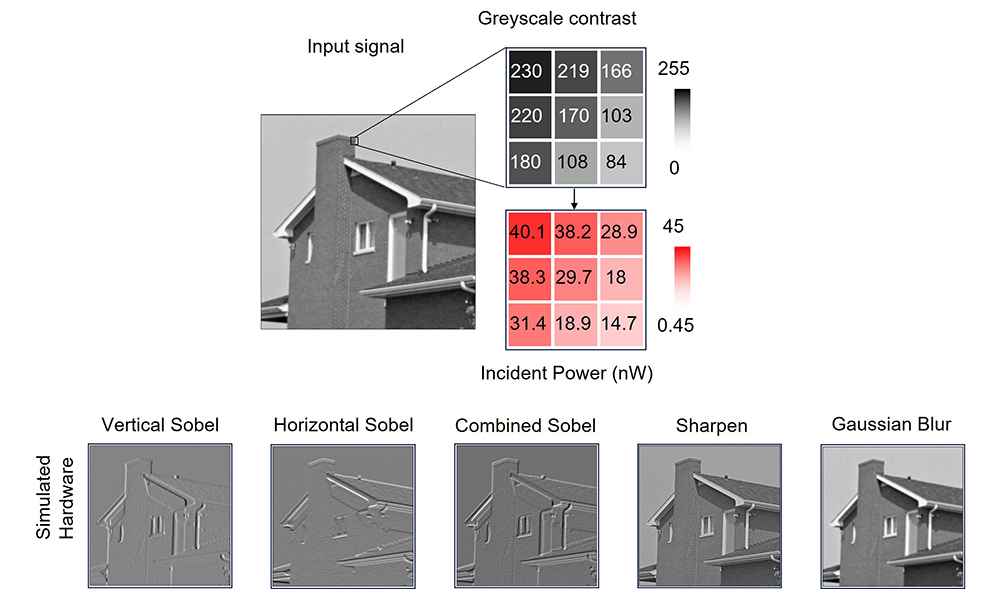
1D and 2D integrations provide significant promise for machine vision by enabling compact, power-efficient optoelectronic devices. However, the potential of 1D materials in mixed-dimensional structures for convolutional image processing remains largely unexplored. Here, high-quality 1D- Nb2Pd3Se8 is synthesized and integrated with 2D-WSe2 to form self-powered photodetectors, exhibiting gate-tunable bi-directional photoresponse for image processing. Utilizing the narrow band gap and favorable work function of 1D- Nb2Pd3Se8, a type-I junction and 1D van der Waals interface are established with transition metal dichalcogenides. The gate tunable built-in electric field enables switching between n-p and n-n+ configurations, allowing the drift photocurrent direction to be reversed, achieving both negative and positive photocurrent. Furthermore, efficient conversion of high-energy photons along one dimension enhances sensitivity at 375 nm. The device achieves a responsivity of 232 mA W-1, external quantum efficiency of 77% at 375 nm illumination, rapid response time of ~3 µs, detectivity of 6.35 × 10¹⁰ Jones, and broadband photodetection from ultraviolet to near-infrared. The demonstrated gate-controllable, bi-directional photoresponse with linear power dependence in a 1D heterojunction offers a promising platform for in-sensor convolutional processing with high integration and portability.
- Author (Pusan National University): Ji-Hee Kim (Department of Physics)
- Title of original paper: Van der Waals integration of 1D Nb2Pd3Se8 and 2D WSe2 for gate-tunable in-sensor imaging processing
- Journal: Advanced Materials
- Web link: https://doi.org/10.1002/adma.202500011
- Contact e-mail: kimjihee@pusan.ac.kr

 951김지희교수1.jpg
(245KB)